Investigating the Scaling Effects on SRAM Data Retention Voltage
Overview
This project investigated how technology scaling impacts the data retention voltage (DRV) of SRAM cells, a key factor in leakage power reduction for low-power VLSI systems. Since SRAM standby leakage can dominate system power in battery-powered devices, minimizing DRV is essential for extending battery life while ensuring memory stability.
Our work explored both analytical modeling and circuit-level simulations to quantify DRV under different transistor sizing and technology parameters.
Problem Context
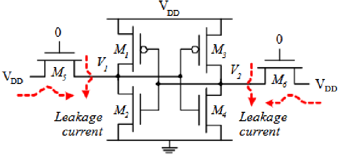
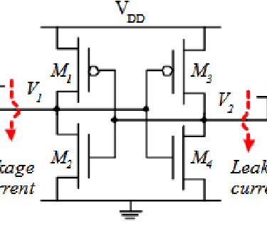
A Static Random-Access Memory (SRAM) is a type of volatile memory capable of storing one bit of data as long as power is supplied. A standard SRAM cell is typically implemented using six CMOS transistors—comprising two PMOS and four NMOS transistors. In this configuration, the PMOS transistors function as pull-up devices, while the NMOS transistors serve both as pull-down elements and as access switches between the bit lines and the memory cell.
SRAM operates in three distinct modes: write, hold, and read. During the write operation, four transistors are active regardless of whether a logic '0' or '1' is being written. In the hold state, two transistors remain active to maintain the stored data. During the read operation, four transistors are switched on to allow data access.
As integrated circuit technology continues to scale down, leakage power consumption has become a major challenge in low-power VLSI (Very Large-Scale Integration) design, especially in on-chip SRAM (Static Random-Access Memory).
This is particularly problematic for battery-powered systems. In such systems, SRAM leakage during standby mode can dominate total system power consumption, threatening battery life and operational efficiency.
A promising technique to mitigate this is reducing the standby supply voltage (VDD) to the lowest possible value at which data is still retained — known as the Data Retention Voltage (DRV).
Methodology
1. Determining DRV through Simulation
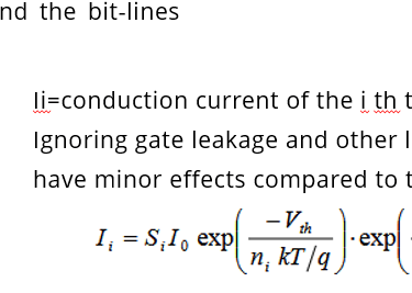
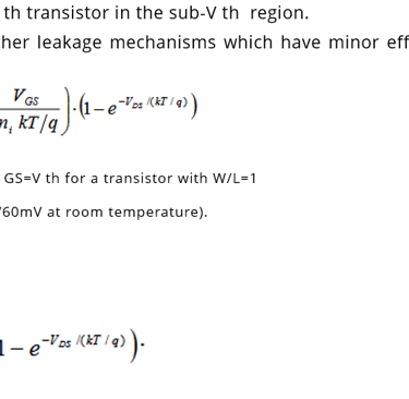
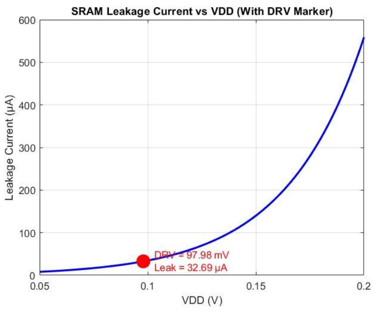
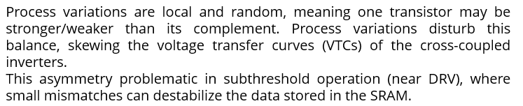
When VDD is reduced to DRV, all six transistors are in the sub-threshold region. Data retention depends strongly on sub-threshold conduction. At DRV, the voltage transfer curves of the inverters degrade until the noise margin falls to zero.
The DRV is found by solving the subthreshold VTC equations of the inverters, considering that all transistors are in weak inversion when VDD is around DRV.
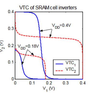
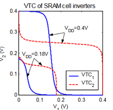
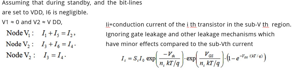
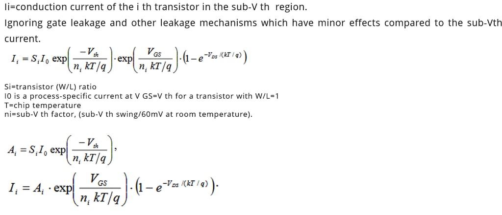
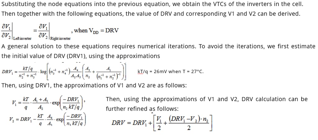
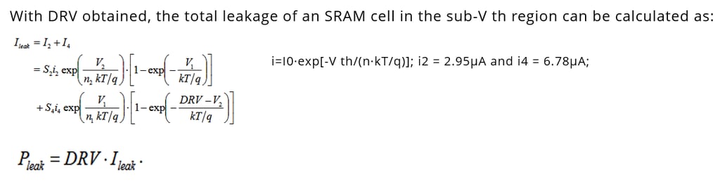
Using the above equations, the DRV was calculated using Matlab.
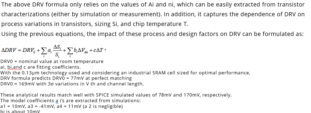
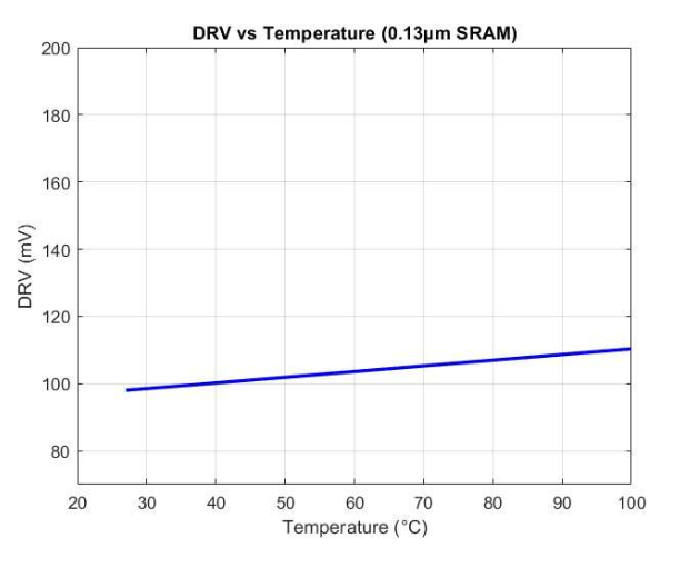
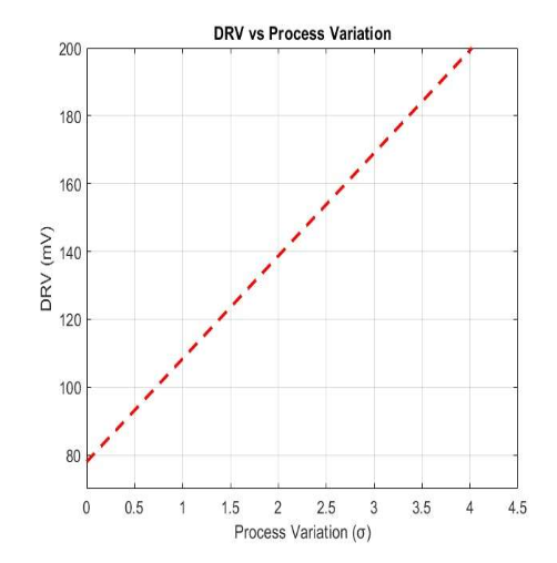
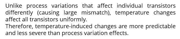
2. Investigating Effect of Process Variation and Temperature on DRV
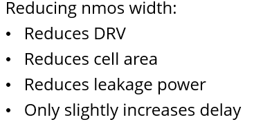
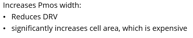
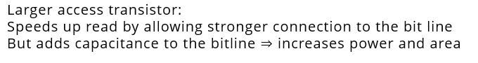
2. Design Tradeoff Analysis
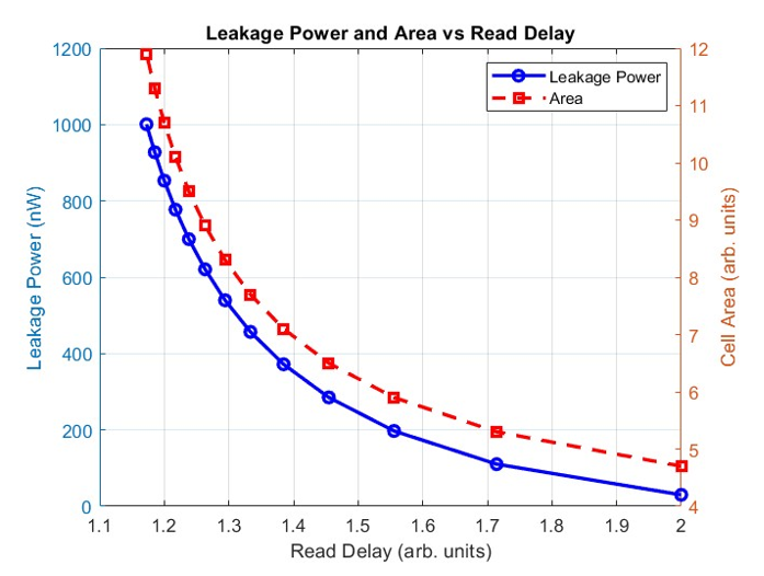
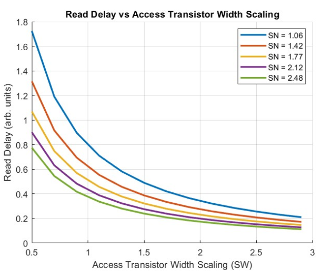
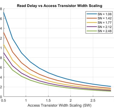
Strategy:

Final Thoughts
I gained hands-on experience with analytical modeling, SPICE validation, and exploring the effects of scaling on SRAM reliability. By balancing trade-offs in leakage, delay, stability, and area, I built a solid foundation in low-power VLSI and memory design—skills essential for advancing modern semiconductor and system-on-chip technologies.
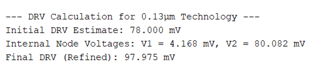
We found the initial estimate of DRV from Spice simulation.
Connect
Explore my projects and coursework for insights.
afiah468@gmail.com
+970-689-1697
© 2025. All rights reserved.