8 Bit Asynchronous Multiplier
Overview
This project focused on the design and implementation of an 8-bit asynchronous multiplier optimized for speed, reliability, and manufacturability. The multiplier was engineered to handle input data rates up to 1 MHz, drive a 1 pF load capacitance, and include an asynchronous global clear signal for robust system resets. By incorporating a 16-bit output architecture, the design ensures overflow prevention while maintaining accuracy and efficiency—demonstrating its suitability for real-world, high-performance electronic systems.
Objectives
Develop a high-speed 8-bit asynchronous multiplier.
Integrate a global asynchronous clear/reset signal (active-low).
Ensure robust 16-bit outputs to prevent overflow.
Optimize for low power consumption and timing accuracy.
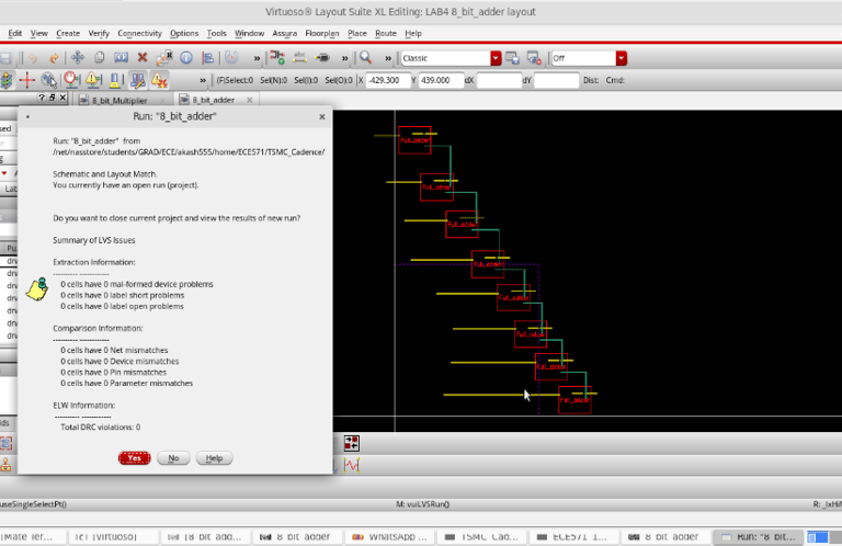
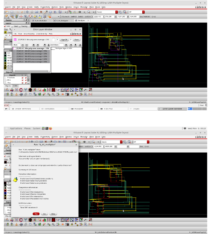
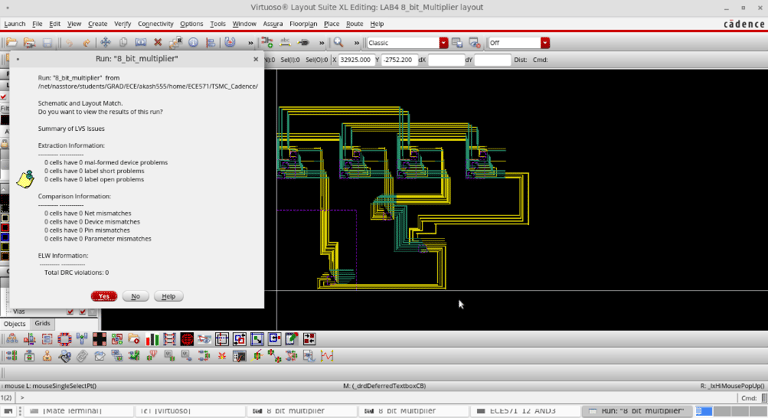
Verify schematic and physical layout with industry-standard design checks (DRC, LVS).
Methodology
1. Schematic Design
Designed and simulated core building blocks (full adders, flip-flops, multipliers).
Optimized library cell selection and gate sizing for speed and efficiency.
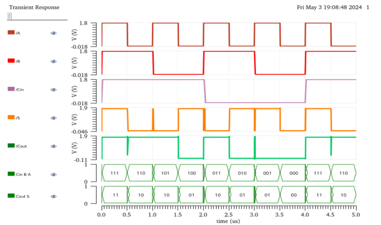
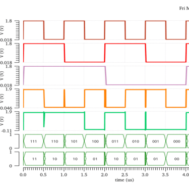
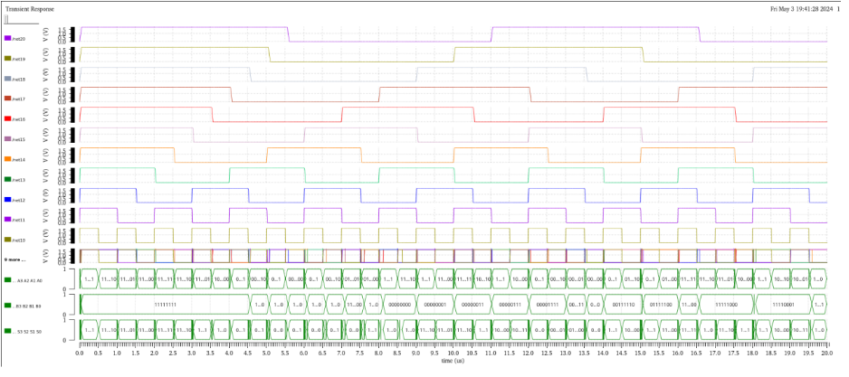
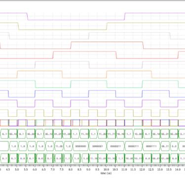
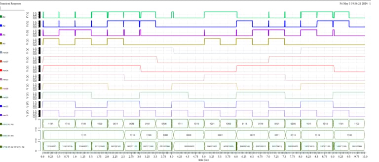
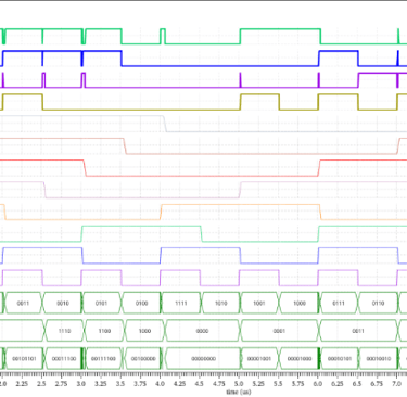
Verified functional correctness through waveform simulations.
2. Layout Design
Implemented the physical layout using Cadence tools with strict 3-metal-layer limits.
Performed manual optimizations to minimize parasitic effects and improve signal integrity.
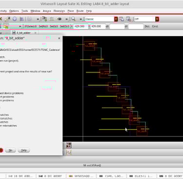
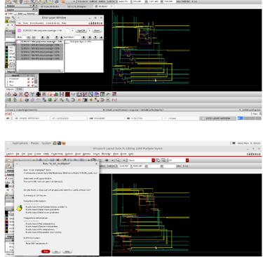
Conducted DRC, LVS, and ERC checks to ensure manufacturability and reliability.
3. Verification & Testing
Confirmed 1 MHz input handling without timing errors.
Validated global SET/RESET functionality for robust operation.
Ensured accurate 16-bit output under all test conditions.
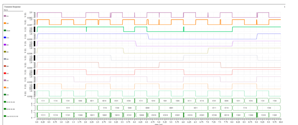
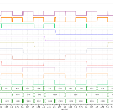
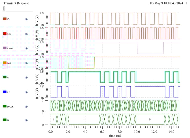
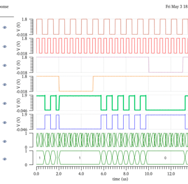
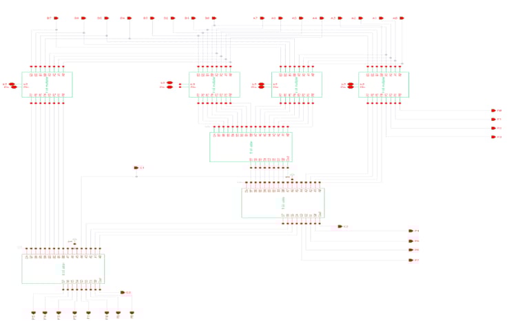
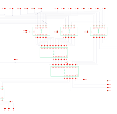
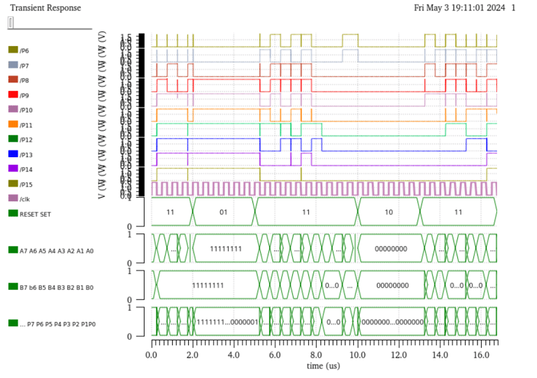
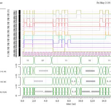
Schematics and Waveforms
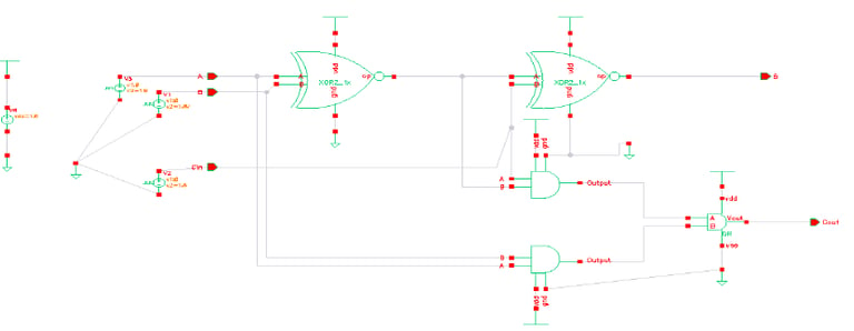
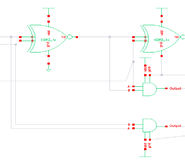
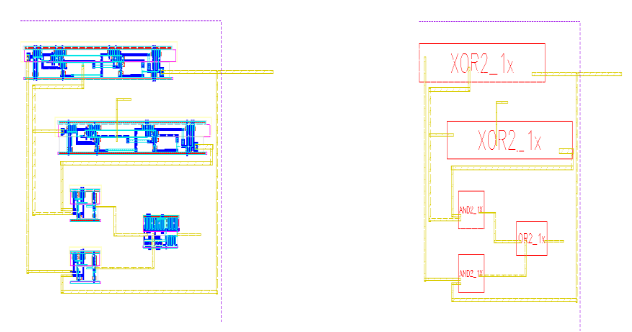
1. Full Adder
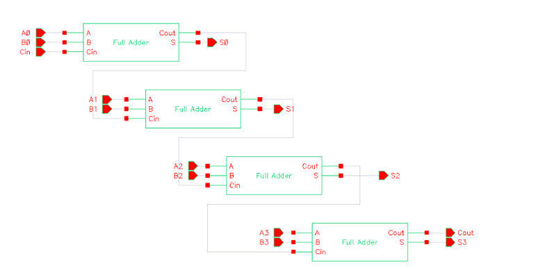
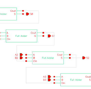
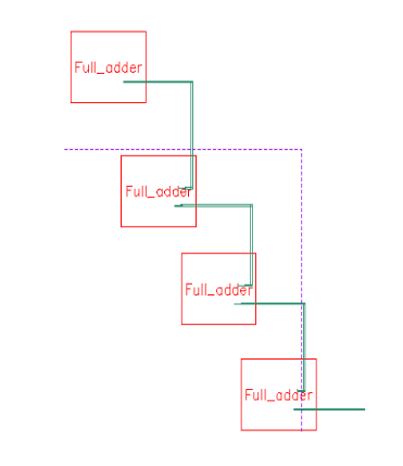
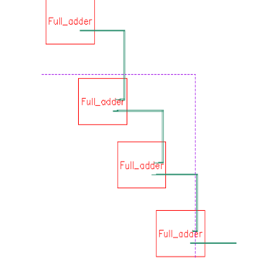
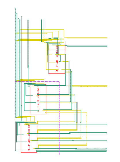
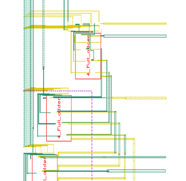
2. 4 Bit Full Adder
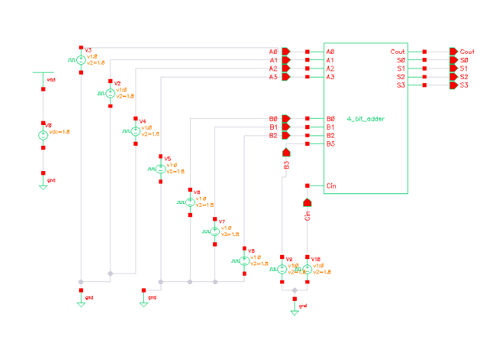
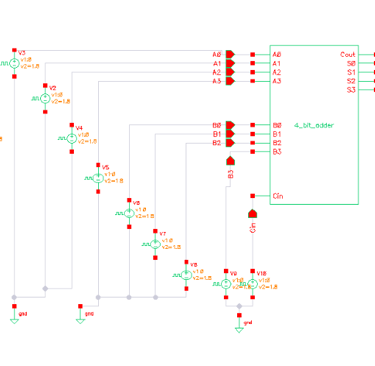
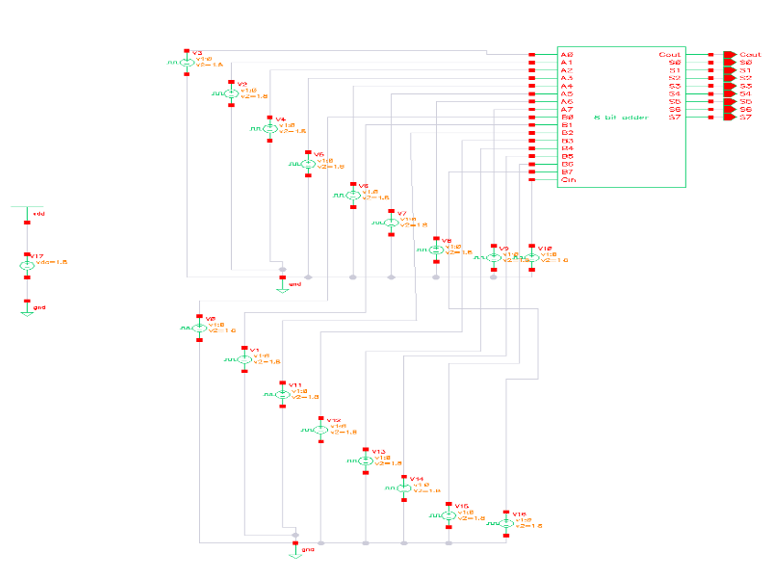
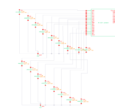
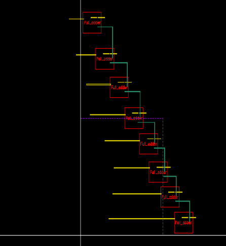
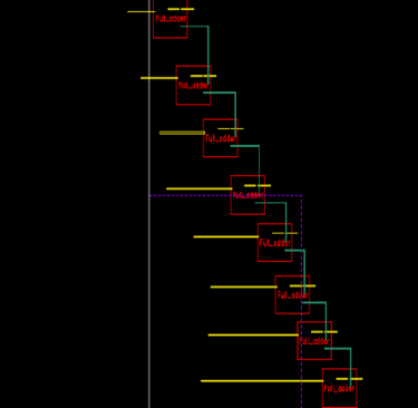
3. 8 Bit Adder
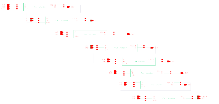
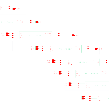
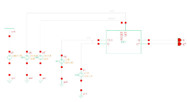
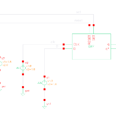
4. D Flip Flop
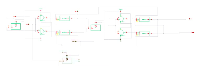
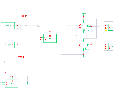
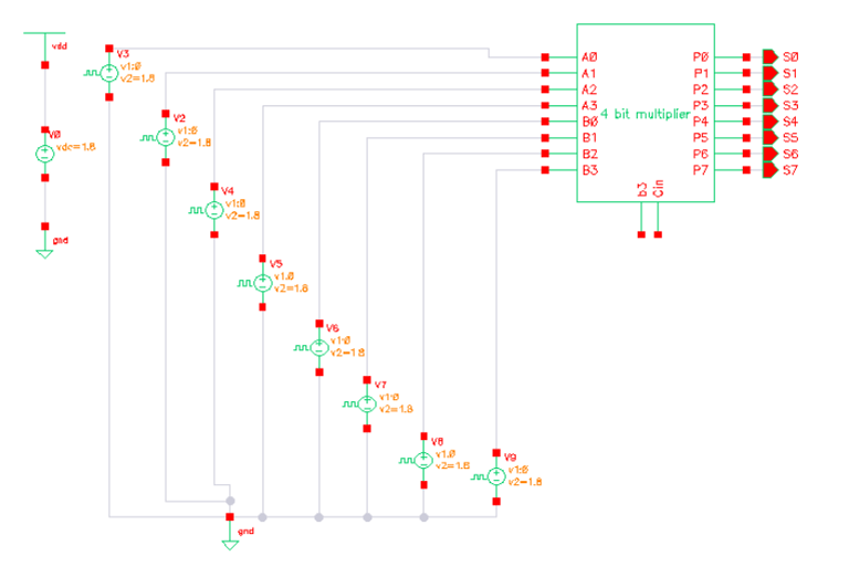
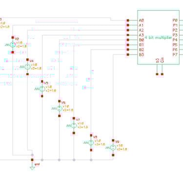
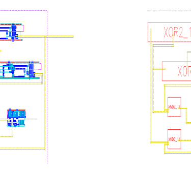
5. 4 Bit Multiplier
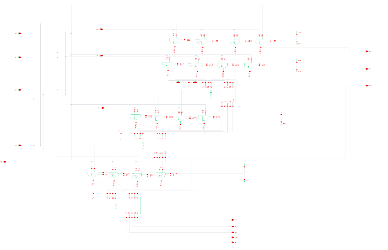
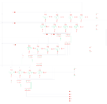
6. 8 Bit Multiplier
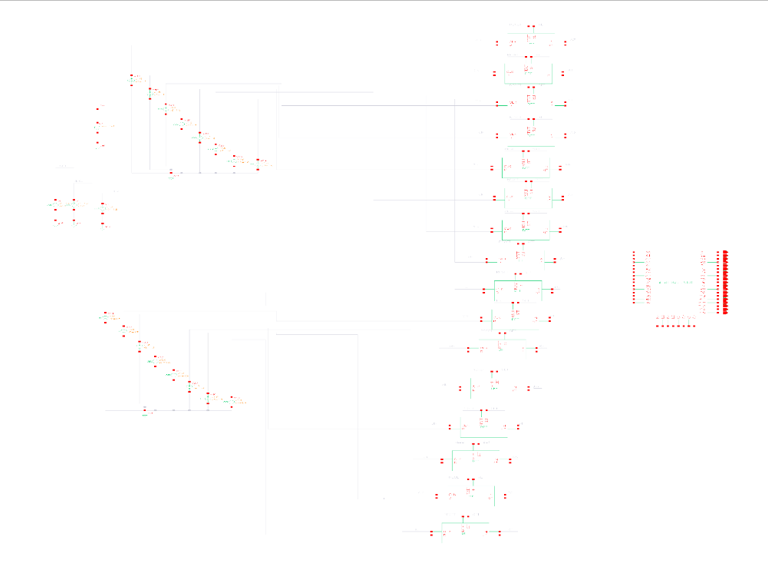
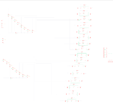
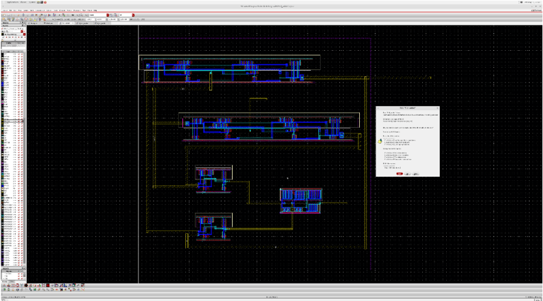
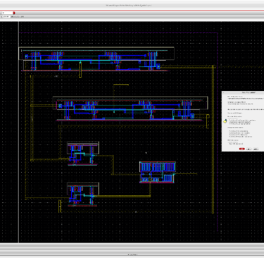
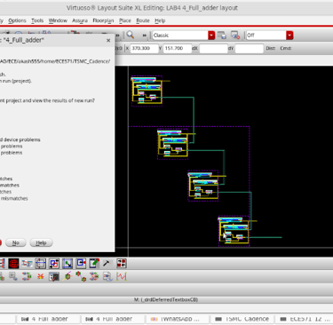
Layouts and Testbench
1. Full Adder Layout
2. 4 Bit Full Adder Layout

3. 8 Bit Full Adder Layout
4. 4 Bit Multiplier Layout
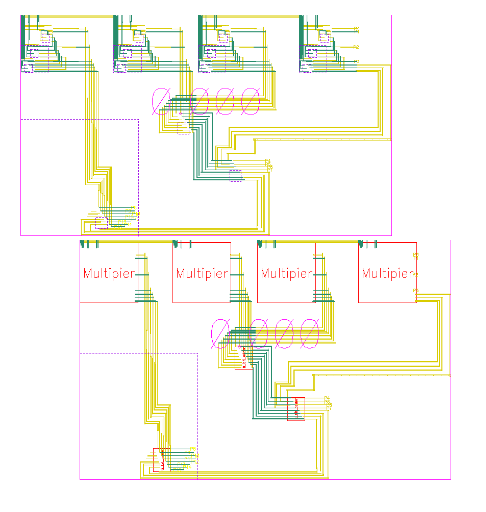
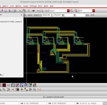
5. 8 Bit Multiplier Layout

Final Thoughts
Results
High Reliability: Stable operation with no glitches during asynchronous reset.
Performance Accuracy: Successfully processed inputs at 1 MHz without delays.
Data Integrity: Maintained 16-bit output accuracy with no overflow issues.
Robust Layout: Optimized routing, minimized parasitics, and confirmed compliance with fabrication rules.
This project challenged my ability to take a digital circuit from schematic to verified physical layout, balancing performance, power, and manufacturability. By combining automated layout generation with manual design optimizations, I ensured that the multiplier met stringent requirements and was ready for real-world application.
Connect
Explore my projects and coursework for insights.
afiah468@gmail.com
+970-689-1697
© 2025. All rights reserved.